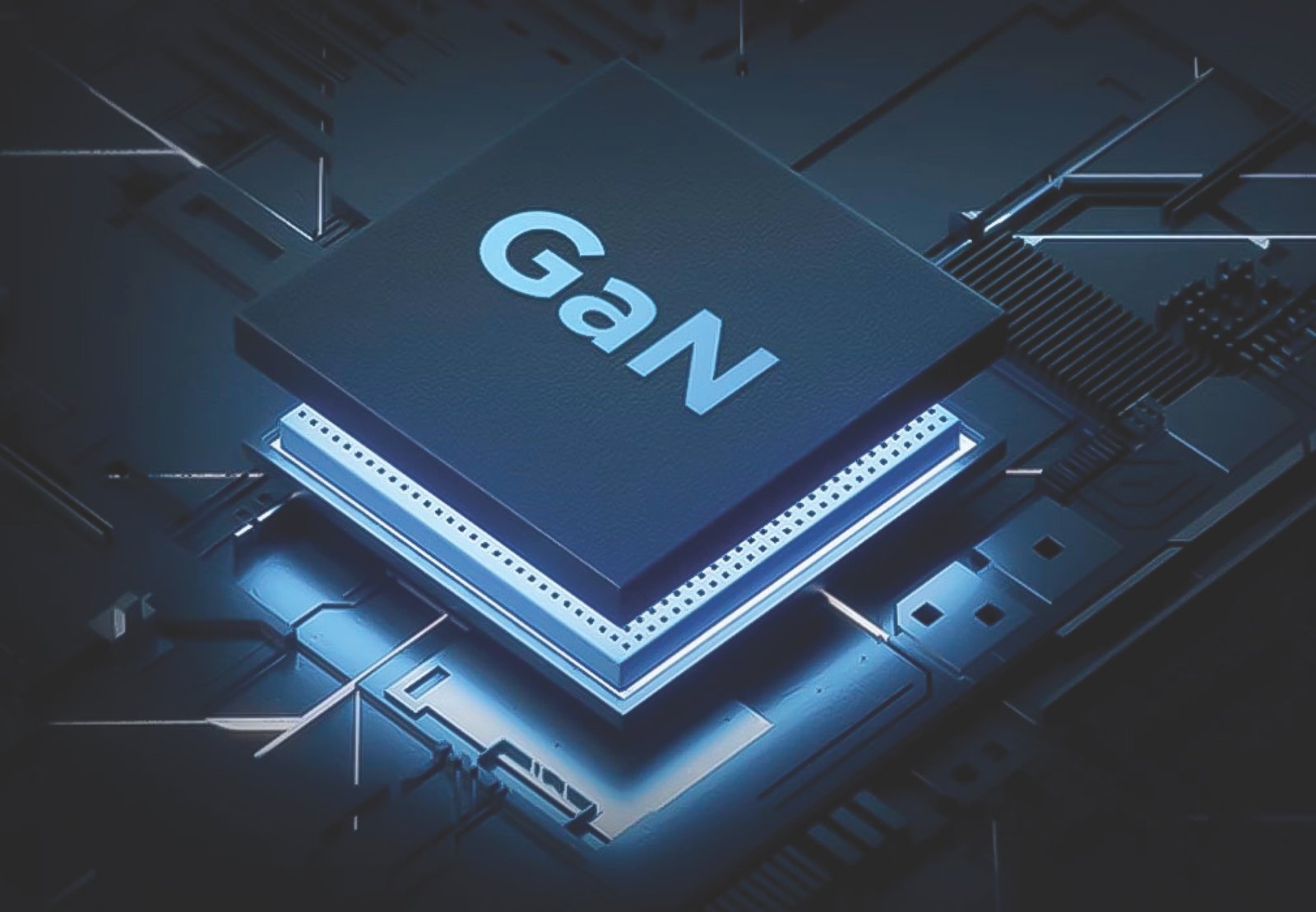
GaN, a technology inflection point
1. Infineon pioneers the world's first 12-inch(300mm) GaN wafer.
Recently, Infineon announced that it can produce chips made of the innovative material gallium nitride at a lower cost, the company has successfully developed the world’s first 12-inch (300mm) power gallium nitride (GaN) wafers, and will be presented to the public at the Munich Electronica exhibition in November this year. Infineon hopes to ensure that the price of GaN chips will not be higher than that of silicon semiconductors in the long term through the new process. The technology is said to have been validated on a pilot production line located at the Fierach plant and production capacity will now be expanded in line with demand. As the first company in the world to master this breakthrough technology in an existing scalable high-volume production environment, Infineon’s breakthrough will significantly boost the gallium nitride power semiconductor market. 12-inch wafers can produce 2.3 times more chips per wafer compared to 8-inch wafers, a significant improvement in technology and efficiency.
Infineon said that one of the major advantages of 12-inch GaN technology is that it can utilize existing 12-inch silicon wafer manufacturing equipment, due to the fact that GaN and silicon manufacturing processes are very similar. Infineon’s existing large-scale 12-inch silicon wafer production line is ideal for piloting reliable gallium nitride technology, which is conducive to accelerating the speed of implementation and effective use of funds.
Full-scale mass production of 12-inch GaN production will contribute to cost parity between GaN and silicon at the on-resistance level, which means cost parity for similar silicon and GaN products.
2. Shin-Etsu Chemical Introduces QST Substrate, a New GaN Breakthrough
Shin-Etsu Chemical announces the realization of a GaN-specific growth substrate, the 300mm QST substrate, and the start of sample shipments.A key breakthrough of the 300mm QST substrate is that it has the same coefficient of thermal expansion as GaN, overcoming the large coefficient of thermal expansion (CTE) mismatch between GaN and Si wafers typically used to fabricate GaN power devices. This allows the epitaxial growth of high quality GaN up to 300mm thick without “warpage” or “cracking”.
At present, some customers have begun to use QST substrate and QST epitaxial substrate GaN development of power devices, high-frequency devices and LEDs, and has entered the development stage of the data center power supply.
In addition, the world has Intel, Crystal Cham Semiconductor, IVWorks and many other companies have also announced the realization of 12-inch GaN breakthroughs in the device, epitaxial, production facilities and other aspects of technological breakthroughs.
Driven by the AI wave, data center and embodied intelligence have become important application landing points. For the new material gallium nitride (GaN), in addition to consumer electronics fast charging scenarios, its application market will also rapidly expand. Experts expect that the gallium nitride power semiconductor business will achieve nearly 10-fold growth: from $260 million last year to $2.5 billion in 2029.
Gallium nitride, as the leader of the third generation of semiconductor materials, the current advantage gradually prevail.